
SiT95148
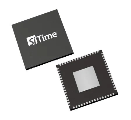
Network synchronizers & jitter cleaners
For network synchronization and jitter cleaning. Compare input/output interfaces, PLL count and operating modes.
PDF · 4.51 MB · 117 pages
| Output frequency | Differential: 8 kHz–2.1 GHz; LVCMOS: 8 kHz–250 MHz; one output supports 1 Hz–2.1 GHz |
|---|---|
| Output | LVPECL, CML, HCSL, LVDS, LVCMOS |
| Supply voltage (V) | 1.8, 2.5, 3.3 |
| Temperature range (°C) | -40 to +85 |
| Package dimensions (mm) | 9x9 mm, 64-pin |
| Input Frequency Range | 8 kHz to 2.1 GHz (differential), 8 kHz to 250 MHz (LVCMOS) |
| Number of Inputs | 4 |
| Number of Outputs | 11 |
| Number of PLL/Clock Domains | 4 PLLs, 4 time domains |
| Operating Mode | Free running, synchronized, holdover |
| Phase Jitter (rms) | 120 fs |
| Programmable loop bandwidth | 1 mHz–4 kHz |
Ranges cover different ordering options; not every combination is available. Interpret jitter and phase noise using the datasheet test conditions.
Related applications
ORAN Distributed Unit
ORAN Distributed Unit:Timing considerations for ORAN Distributed Unit. Timing and synchronization for wireless networks, data centers and high-speed links, with attention to jitter budgets and clock planning.
View details →Fixed Wireless Access (FWA)
Fixed Wireless Access (FWA):Timing considerations for Fixed Wireless Access (FWA). Timing and synchronization for wireless networks, data centers and high-speed links, with attention to jitter budgets and clock planning.
View details →AI/ML Offload Engines
AI/ML Offload Engines:Timing considerations for AI/ML Offload Engines. Timing and synchronization for wireless networks, data centers and high-speed links, with attention to jitter budgets and clock planning.
View details →FPGA Clocking
FPGA Clocking:Timing considerations for FPGA Clocking. Timing and synchronization for wireless networks, data centers and high-speed links, with attention to jitter budgets and clock planning.
View details →Data checked: 2026-10-27