
SiT91211
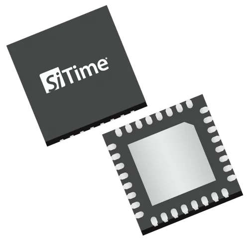
Clock generators
Generate and distribute system clocks. Review output frequencies, channel counts and programming options.
PDF · 1.49 MB · 28 pages
| Output frequency | 1 to 700 MHz (differential) 1 to 220 MHz (LVCMOS) |
|---|---|
| Frequency stability | ±20 ppm (-40°C to 105°C), ±50 ppm (-40°C to 105°C) |
| Output | LVDS , LPHCSL LVPECL , LVCMOS |
| Supply voltage (V) | 1.8, 2.5, 3.3 |
| Temperature range (°C) | -40 to 85, -40 to 105 |
| Package dimensions (mm) | 4x4 mm, 24-pin QFN |
| Phase Jitter (rms) | 150 fs (typ.) |
| PCIe Support | Gen 1 to Gen 7 |
Ranges cover different ordering options; not every combination is available. Interpret jitter and phase noise using the datasheet test conditions.
Related applications
Fixed Wireless Access (FWA)
Fixed Wireless Access (FWA):Timing considerations for Fixed Wireless Access (FWA). Timing and synchronization for wireless networks, data centers and high-speed links, with attention to jitter budgets and clock planning.
View details →Host Bus Adapter
Host Bus Adapter:Timing considerations for Host Bus Adapter. Timing and synchronization for wireless networks, data centers and high-speed links, with attention to jitter budgets and clock planning.
View details →PAM4 for High-Speed Links
PAM4 for High-Speed Links:Timing considerations for PAM4 for High-Speed Links. Timing and synchronization for wireless networks, data centers and high-speed links, with attention to jitter budgets and clock planning.
View details →FPGA Clocking
FPGA Clocking:Timing considerations for FPGA Clocking. Timing and synchronization for wireless networks, data centers and high-speed links, with attention to jitter budgets and clock planning.
View details →Data checked: 2026-10-27